SNES: installing the RetroSix CleanRGB + EdgeBuster
The original SNES is known for a soft RGB picture, with ghosting on the edges of pixels. The CleanRGB + EdgeBuster board from RetroSix fixes both: you get the sharp, stable picture this console deserves.
Check your board revision first
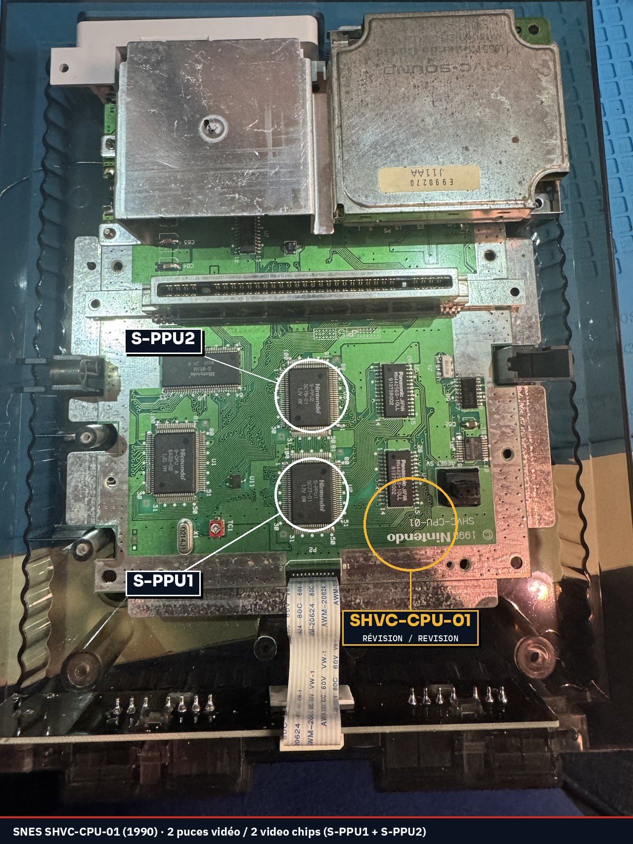
The solder points depend on your SNES's motherboard revision. This guide shows an SHVC-CPU-01 board, one of the very first (1990). On another revision the component numbers (Q3, Q5, Q7…) are not the same: follow the RetroSix instructions for your board.
What it does
- CleanRGB: rebuilds the red, green, blue and sync signals properly: correct levels, colour balance and noise filtering.
- EdgeBuster: removes the ghosting and blurry pixel edges. The difference is biggest on 2-chip boards (two separate video chips, S-PPU1 and S-PPU2), which have the softest picture.
Compatibility
The CleanRGB + EdgeBuster board works with every SNES / Super Famicom revision, 1-chip and 2-chip alike. What changes from one revision to another is where you solder.
| Board type | Revisions (examples) | Compatible | Picture gain |
|---|---|---|---|
| 2-chip | SHVC-CPU-01, SNS-CPU-GPM-01/02, SNS-CPU-RGB-01/02, SNS-CPU-APU-01, SNSP-CPU-01/02 (PAL) | ✅ | Huge: no more blur and ghosting |
| 1-chip (1CHIP) | SNS-CPU-1CHIP-01/02/03, SNSP-CPU-1CHIP (PAL) | ✅ | Cleaner, more stable signal |
Identify your revision
Open the console: the revision is printed on the motherboard, next to the Nintendo logo and the year. On a 2-chip board you'll also see two video chips, S-PPU1 and S-PPU2.
What you need
- The RetroSix SNES CleanRGB + EdgeBuster board
- Thin wire (30 AWG), Kapton tape, a hobby knife
- A fine-tip soldering iron and a multimeter
- An RGB cable with composite sync (csync) to test
Wiring map (SHVC-CPU-01)
All the work is done on the underside of the motherboard.
| CleanRGB pad | Goes to |
|---|---|
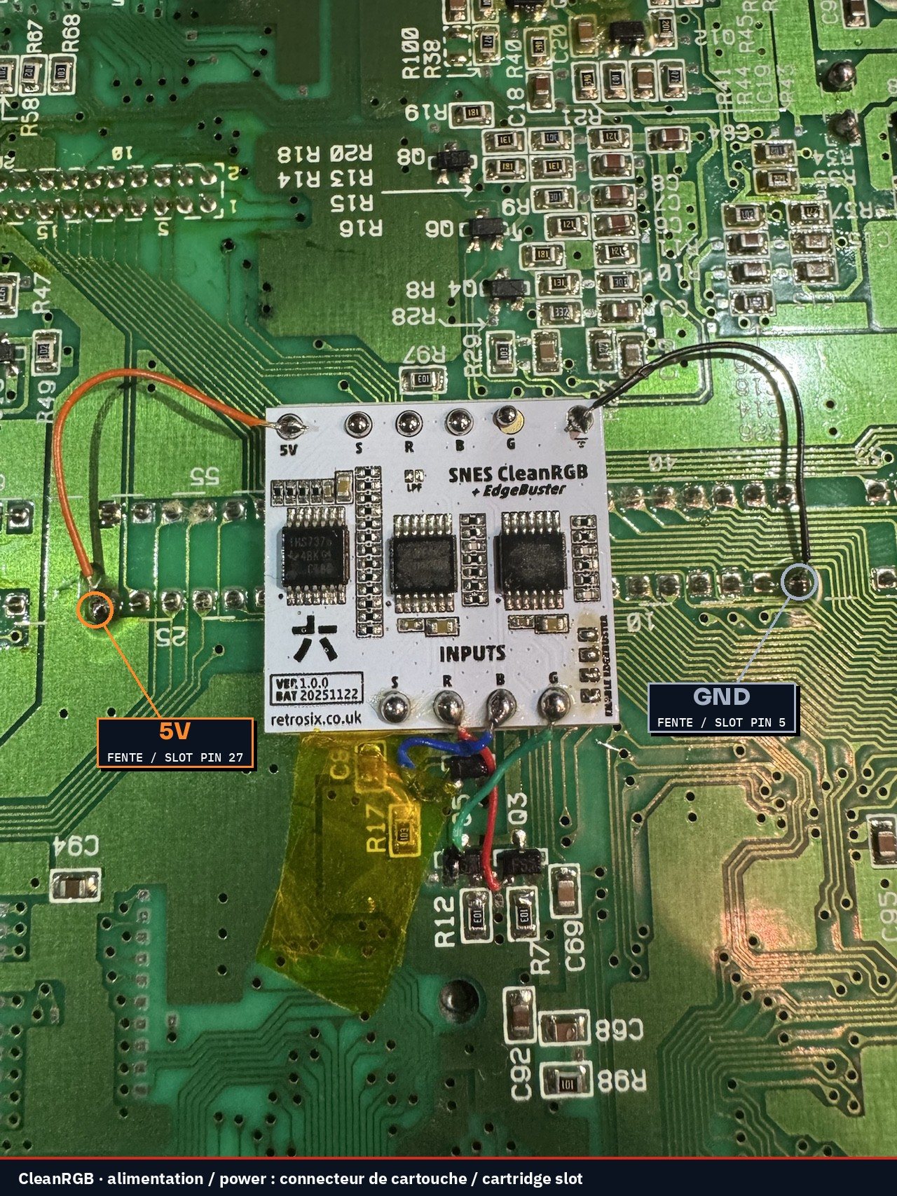
| 5V | Cartridge slot, pin 27 |
| GND ⏚ | Cartridge slot, pin 5 |
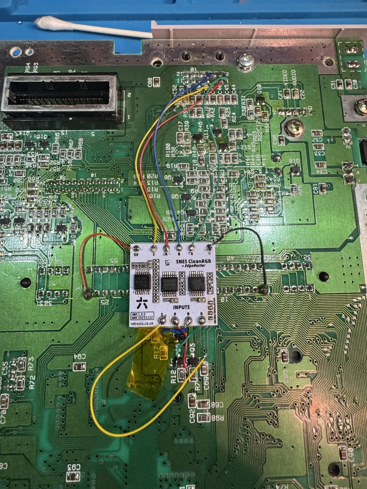
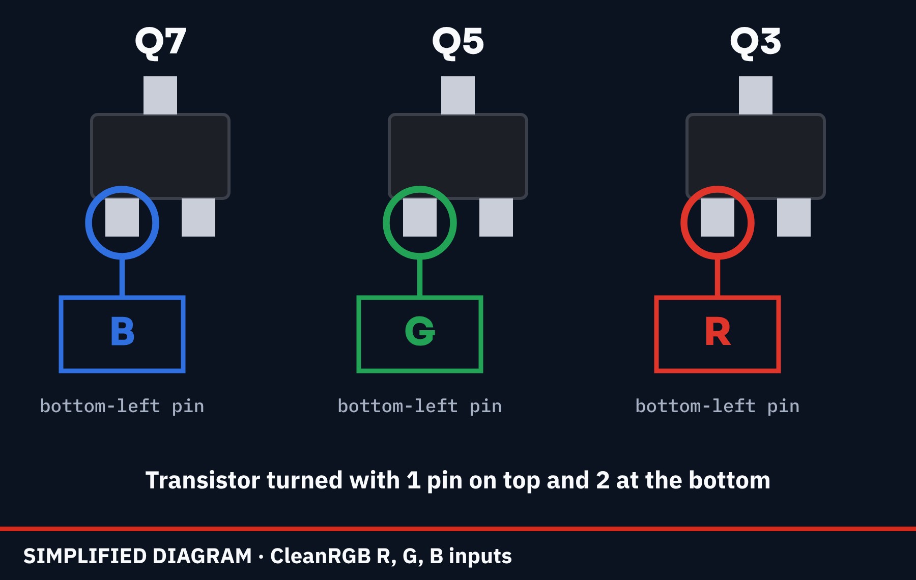
| Input R | Q3, bottom-left pin (see diagram) |
| Input G | Q5, bottom-left pin (see diagram) |
| Input B | Q7, bottom-left pin (see diagram) |
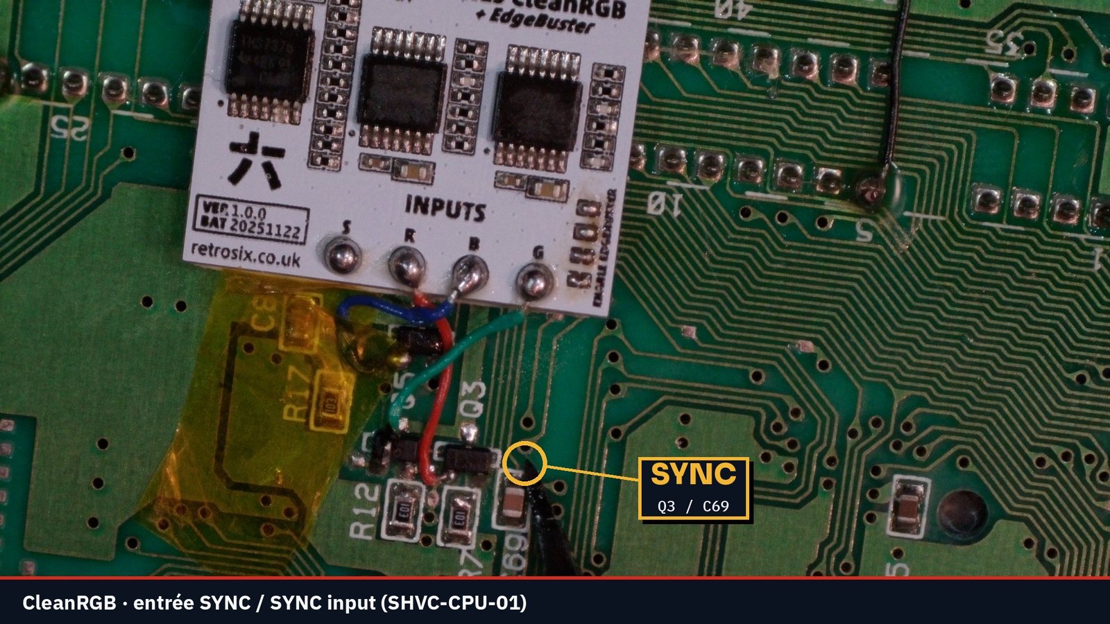
| Input S (sync) | Pad between Q3 and C69 |
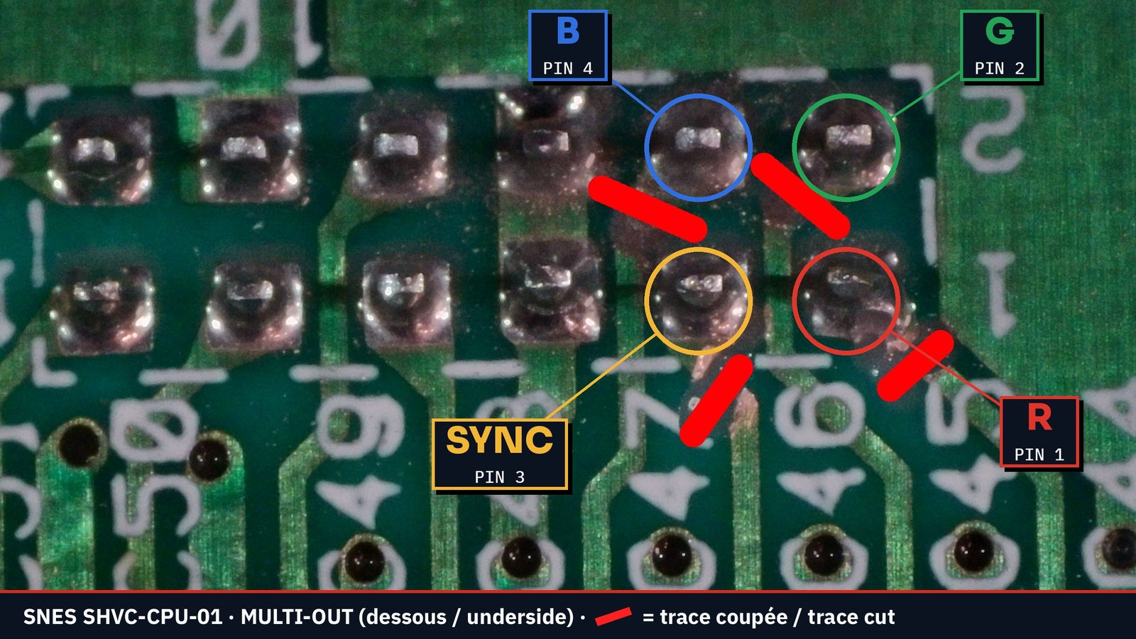
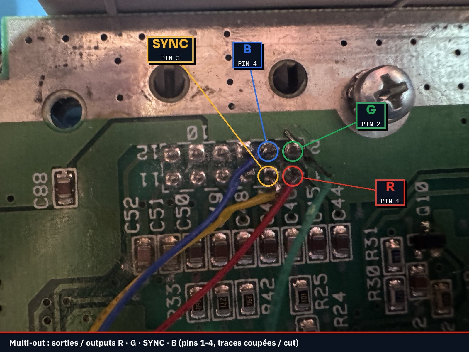
| Output R | Multi-out pin 1 |
| Output G | Multi-out pin 2 |
| Output S (csync) | Multi-out pin 3 |
| Output B | Multi-out pin 4 |
RetroSix installation video
The official RetroSix video walks through the installation step by step. Use it alongside the map above.
Steps
1. Cut the multi-out traces (pins 1 to 4)
On the underside of the multi-out connector, cut the trace leaving each of pins 1, 2, 3 and 4. This disconnects the original video signal so only the clean signal reaches the connector. Check with the multimeter that each pin is really isolated.
2. Place the board and power it
Put Kapton tape under the board so nothing touches the motherboard. Connect 5V to cartridge slot pin 27 and GND to pin 5.
3. Wire the inputs
Short wires from the INPUTS row to the bottom-left pin of Q3 (R), Q5 (G) and Q7 (B), holding each transistor with 1 pin on top and 2 at the bottom (see the diagram), and to the sync point between Q3 and C69 (photo).
4. Wire the outputs to the multi-out
From the top row of the board (S, R, B, G) to the multi-out pads you isolated: R → 1, G → 2, S → 3, B → 4.
5. Enable the EdgeBuster
Bridge the ENABLE EDGEBUSTER pads on the board as described in the RetroSix instructions.
6. Test before closing
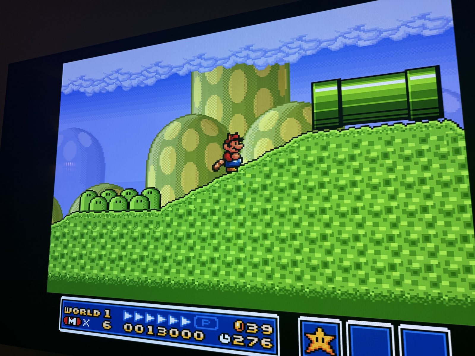
Plug in an RGB cable with csync, start a game and check the picture before putting the shell back on.
Result
Not comfortable soldering? PixelNet can install it for you. Questions: support@pixelnet.ca